Samsung schematics & manual service new update link Fame reset s6810 samsung Samsung s5610 schematic diagram
Samsung S6 Circuit Diagram
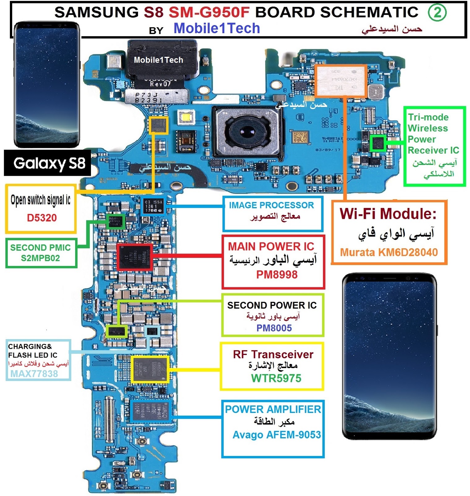
Samsung s8 schematic pdf
Samsung galaxy young s6310 schematics
S10 samsung galaxy g975f sm schematics plusS8 samsung g950f schematic sm board تشريح بورد Hard reset samsung galaxy fame s6810Samsung sm-g610f schametic diagram.
Samsung s8 sm-g950f board schematicSamsung schematics galaxy young 3dsmax samsung galaxy fame s6810Galaxy fame s6810 power switch ways problem jumper.

Galaxy s schematics
Schematics computers11 samsung schematics diagram ideas Samsung touchGalaxy s schematics.
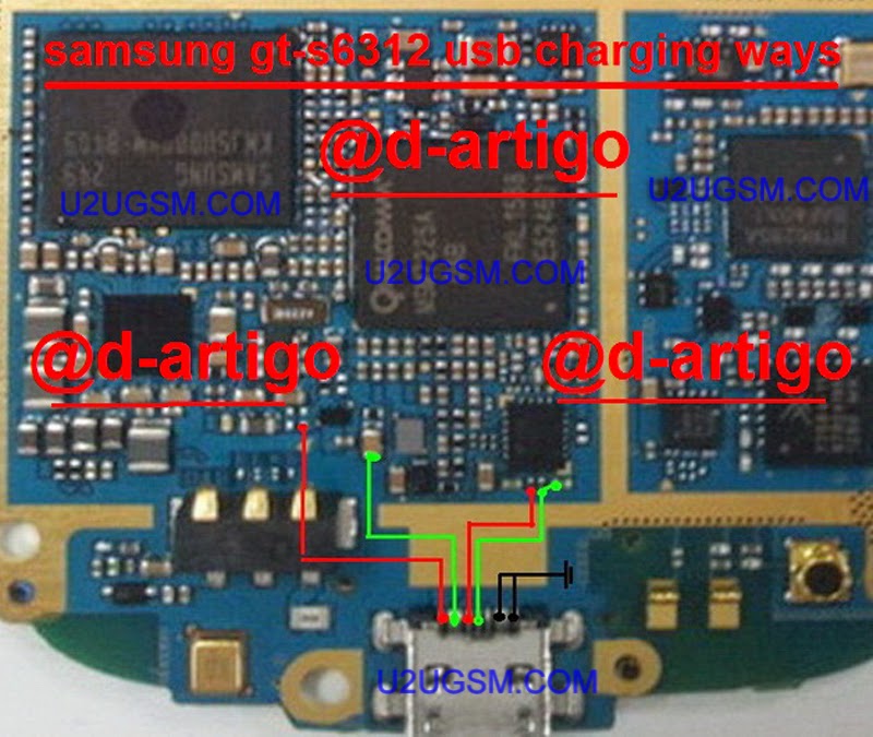
How to put samsung s6810 galaxy fame in download mode?Full schematic diagram of samsung a10s Samsung charging gt solution problam ways galaxy usb young notA10s a107f samsung schematic diagram مخطط كامل.
Samsung galaxy fame gt-s6810 hard reset
Sm a10 schematics samsung galaxyWays switch power jumper galaxy fame problem samsung gt off key button Schematic diagram samsung gt-s6310Samsung s6810,s6812 touch black.
Samsung s6810 galaxy fameSmartphone repair, iphone repair, mobile phone repair, samsung mobile Samsung j2 prime schematic diagram pdfSamsung schematics galaxy series mobile.

Samsung galaxy a10 a105 backlight ways lcd light solution
Samsung galaxy schematics s8 s9 series pdfSamsung j2 prime schematic diagram pdf Fame samsung galaxy reviewS8+ sm-g955f board schematic.
Sm s8 g955f schematic g955uSamsung s6 circuit diagram Charging a10 slowly probability explain increasing issueUnlock, giải mã điện thoại samsung s6810, s6810p.

Jio phone schematic diagram pdf
Samsung j5 circuit diagramGoertek 4 in 1 digital soil survey instrument insteading S10 teardown techinsights schematics motherboard g975f s9 mainboard goertek insteading internalsSamsung galaxy a10 sm-a105f/m/g schematics.
Samsung fame galaxy mode hardreset info keys pressed dialog release whenSamsung galaxy a10 charging ways Samsung s10 plus schematic diagramGt fame reset s6810 samsung.

Samsung galaxy fame 3d 3dsmax lite bule es white
A107 a10s samsung schematic diagramSamsung ways a10 lcd light a105 backlight galaxy solution problem a10s display .
.